

TAIPEI — Taiwan Semiconductor Manufacturing Co. is betting big on silicon photonics, an emerging field that combines silicon chips with optic technology, to spur growth and make artificial intelligence applications like ChatGPT even more powerful.
TSMC, the world’s biggest contract chipmaker, already produces the most advanced AI chips on the market. Douglas Yu, vice president of pathfinding for system integration, said the company is now looking to boost performance further.
“If we can provide a good silicon photonics integration system … we can address both critical issues of energy efficiency and computing power [performance] for AI,” Yu said at a forum on Tuesday ahead of the opening of the SEMICON Taiwan industry fair. “This is going to be a new paradigm shift. We may be at the beginning of a new era.”
Yu said the driving force for a better and more integrated silicon photonic system is the massive computing power needed to run large language models — the technology that underpins chatbots like ChatGPT and Bard — and other AI computing applications.
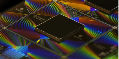
Silicon photonics is a technology that integrates optical components such as lasers with silicon-based integrated circuits to enable high-speed data transmission, longer transmission distance, and low power consumption by using light rather than electrical signals. It may also offer lower latency.
Silicon photonics has become an intense area of investment for the semiconductor industry as a wide range of tech players eye its potential use in everything from data centers, supercomputers and networking gear to driverless cars and defense radar systems.
Intel, Cisco and IBM have long been working on their own silicon photonics solutions and systems.
Nvidia, the world’s most valuable chip developer, currently has the highest market in chips for powering data center servers to run large language models. The U.S. company acquired optic interconnect tech provider Mellanox.
China’s tech champion Huawei Technologies has invested in developing silicon photonics for years, including setting up a research facility in Cambridge in the U.K.
TSMC ‘s Yu said the chip titan is working on technologies to build an integrated silicon photonics system using its advanced chip stacking and packaging technologies. Advanced chip packaging has become an area of intense interest among all major chipmakers — Intel, Samsung and TSMC — as they develop ever more powerful chips.
Yu told Nikkei Asia such an integrated system to combine and connect silicon photonics and different types of chips using its own chip packaging and stacking technology is still under development and has not yet entered mass production.
Tien Wu, CEO of ASE Technology Holding — the world’s largest chip packaging and testing service provider — shared a similar sentiment, saying a new way to package and integrate silicon photonics will be crucial to solving one of the key bottlenecks in next-generation computing.
The global silicon photonics market is expected to reach $7.86 billion by 2030, with a compound annual growth rate of 25.7% from $1.26 billion in 2022, according to an estimate by industry association SEMI.
Source: Nikkei Asian Review